Products
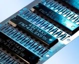
Semiconductor manufacturing processes call for fast and precisely controllable marking solutions. Marking speeds of over 1000 characters/second and material penetration depths of less than 25 µm/1 mil are common.

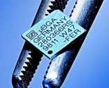
VISION's laser markers generate characters at sizes precisely in accordance with the user's requirements. Even at a character height of 0.2 mm they still ensure best quality. Line widths are selectable from less than 30 µ to more than 160 µ, with controlled material penetration depths of less than 25 µm/1 mil.

With its high accuracy and minimal heat input the laser marks even the smallest parts without any risk of damage. The smaller the parts, the more the laser marker shows its strengths. Depending on the type of material, frequency-doubled or -tripled beam sources will be used as well.

The laser marking of silicon wafers facilitates traceability of the manufacturing process for fault analysis of semi-conductor devices. A laser system designed for wafer marking must meet the most stringent requirements. Thus, the marking must be machine-readable, miniaturized and have no negative influence on the further manufacturing steps and still permit clear identification at the end of the process chain.

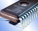
Our broad product range of solid state lasers offers also perfect solutions for marking ceramics. With optimized laser power and beam quality, high-contrast laser markings can be produced at high speed.
For this application we recommend the laser marking machine : VISION EMBESOFT SOLUTION’s LASER MARKING MACHINE
Contact us +91 7575806266 Email : sales@vesindia.org, bhavesh.pethani@gmail.com
| Home | Business Profile | Products | Blog | News | SiteMap | Contact Us | About Us